TCXO failure analysis
2026-03-06 14:00Backstory
Back in January, the ThunderScope team sent me a PCIe card version of their prototype open hardware oscilloscope.
I was very excited about this, because I was already testing ngscopeclient with a Thunderbolt version of the ThunderScope but the only machines I had with Thunderbolt were laptops. The PCIe card version would be usable with my (much more powerful) desktops, allowing me to really push ngscopeclient and the ThunderScope to its limit. It took a bit of experimenting with external GPU enclosures and such to figure out how to get the ThunderScope to sit out on my lab bench so I wouldn’t need to crawl under the bench and run cables up from the workstation on the floor up to probes on my DUT, but I figured that out easily enough.
After getting the drivers installed I fired up ngscopeclient, cabled channel 1 of the ThunderScope to my Siglent SSG5060X-V vector signal generator, and gave it a 100 MHz unmodulated sinewave to check everything out. Everything looked good until I fired up the FFT in ngscopeclient and saw a peak… at around 106 MHz, and unstable - it was moving slightly up and down.
Just to rule out any issues with the Siglent, even though it had been recently checked against cal standards and was locked to my lab 10 MHz distribution system, I directly measured the 10 MHz outputs from my SRS FS752 GPSDO and my Symmetricom rubidium standard with the ThunderScope. Both showed 10.665 MHz, while in reality they were both 10.0000000000 MHz give or take about 2e-11. So the Siglent was fine, and the ThunderScope’s timebase was 6.6% slower than it should have been.
After a bit of back and forth, I was able to read the PLL lock bit for the ADC clock generator via a debug interface - and it wasn’t locked.
A bit of hardware debug later, I confirmed that the output of the 10 MHz TCXO (ECS-TXO-3225MV-100), which provides the primary timebase for the oscilloscope, was flatlined. The PLL VCO was running wild with no edges to lock to, with the nominally 1 GHz ADC clock hovering around 938 MHz but unstable.
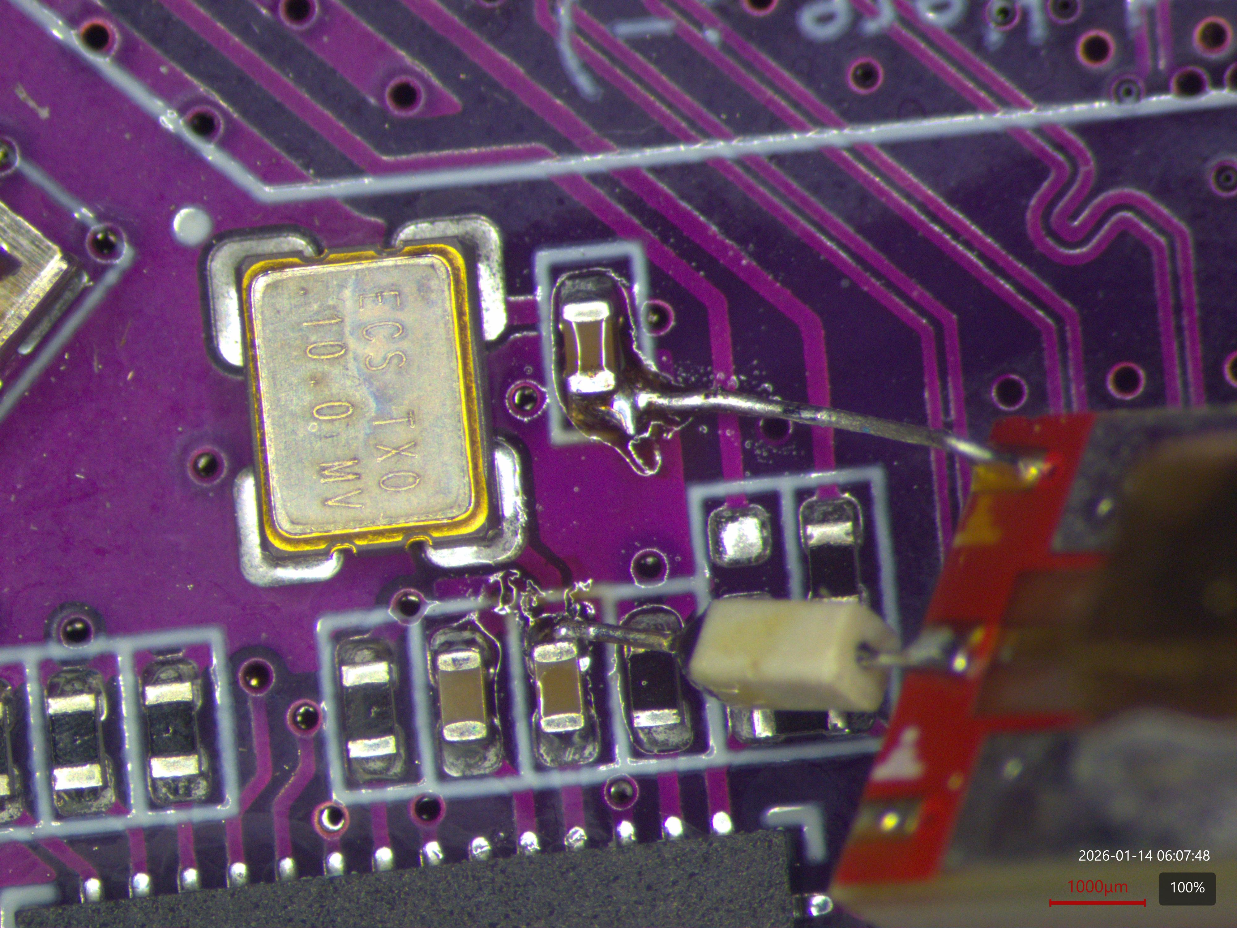
The lack of a PLL reference clock certainly explained why the ThunderScope wasn’t behaving as it should. I reworked the solder joints in case of an assembly defect, but that didn’t solve the problem. So I ordered a new TCXO, swapped the bad one out, and the scope was happy.
Most people would have stopped at this point, but I’m not most people. Why did the TCXO fail?
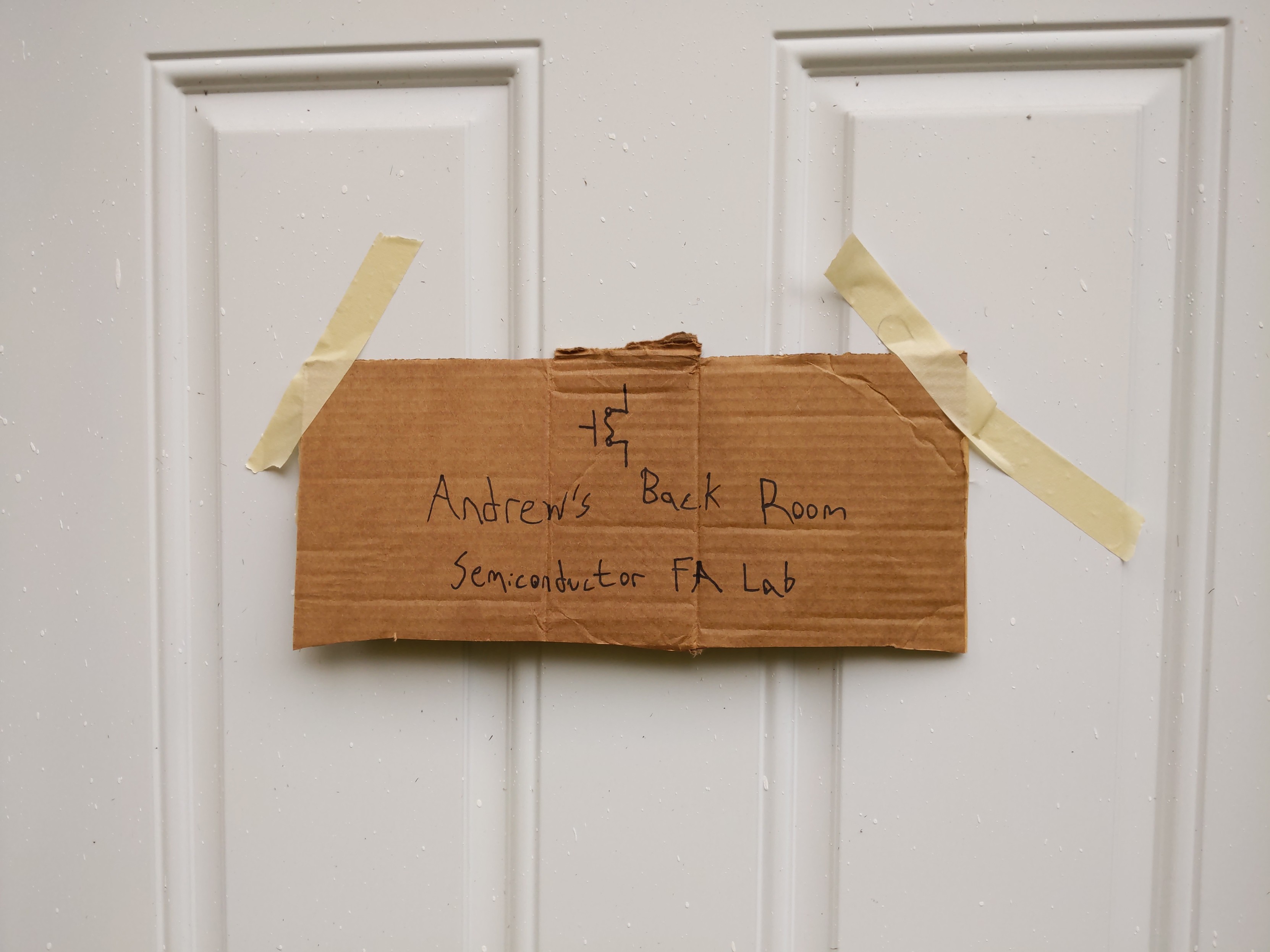
If you’ve been following me for a while, you probably know that I occasionally use my home lab to help friends out when they have failed components and can’t afford to have a “real” IC FA workup done.
Well, thanks to @emily@fedi.uni.horse, Andrew’s Back Room Semiconductor FA Lab now has an appropriately sketchy logo. Now that we’re official, we can get started on the analysis!
What is a TCXO?
First, a bit of background so we know what to expect: a TCXO is a Temperature Compensated Crystal Oscillator (“crystal oscillator” is often abbreviated XO - presumably the X is actually a Greek chi as in Xmas and LaTeX? I’ve never looked into the etymology but that was my first guess).
Normal quartz oscillators drift slightly with changes in temperature, which is bad for precision metrology equipment. A TCXO contains a quartz crystal, an amplifier circuit to drive it, and a temperature compensation circuit which shifts the resonant peak slightly up or down to null out the effects of thermal drift.
So we should expect the device to contain a quartz resonant crystal plus the driver and compensation circuit, which are probably going to be combined into a single integrated circuit. One or both of these, or the connections between them, must have failed in some way since the TCXO isn’t working.
Initial Analysis
After a bit of discussion with Aleksorsist, she mentioned having ultrasonically cleaned the board prior to sending it to me. Sonication of MEMS and oscillators is risky due to the potential for floating structures to resonate at the frequency of the applied ultrasonic energy and be damaged, so I recommended not sonicating future ThunderScopes regardless of whether it ultimately turned out to be the root cause of this device’s failure or not.
The analysis got put on ice for a month or two due to me being very busy at work and dealing with some other higher priority stuff, but yesterday I came across the bad TCXO while cleaning up the lab and decided I had a bit of time to spend poking at it. (That’s a risk you take when you send samples to a back room FA lab, I might forget about them for a while…)
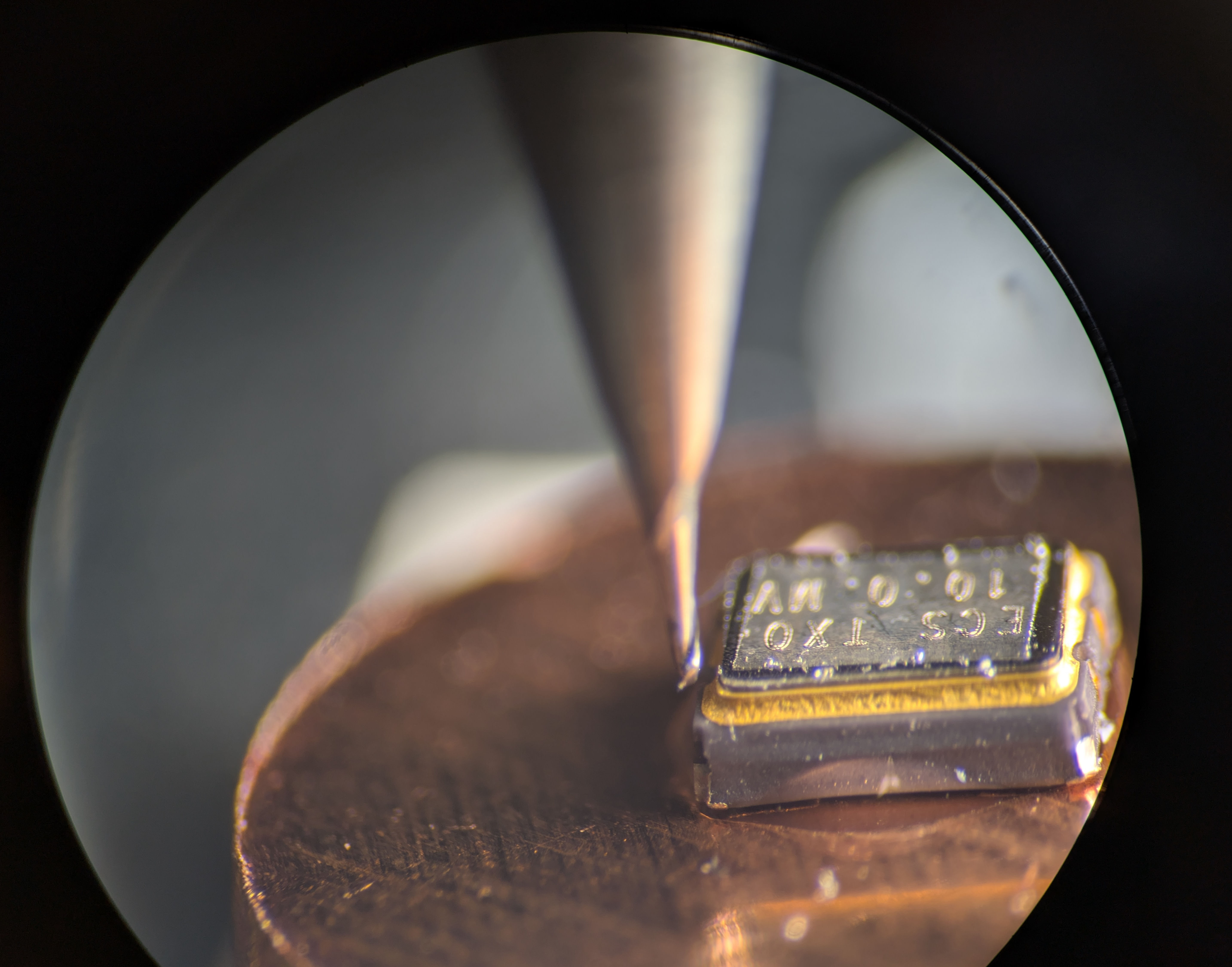
The first step was to clean up the solder and flux residue on the package, then grab top and bottom side photos. Then I used some crystalbond wax to mount it to a copper disk I had lying around the lab so it would be easier to handle.
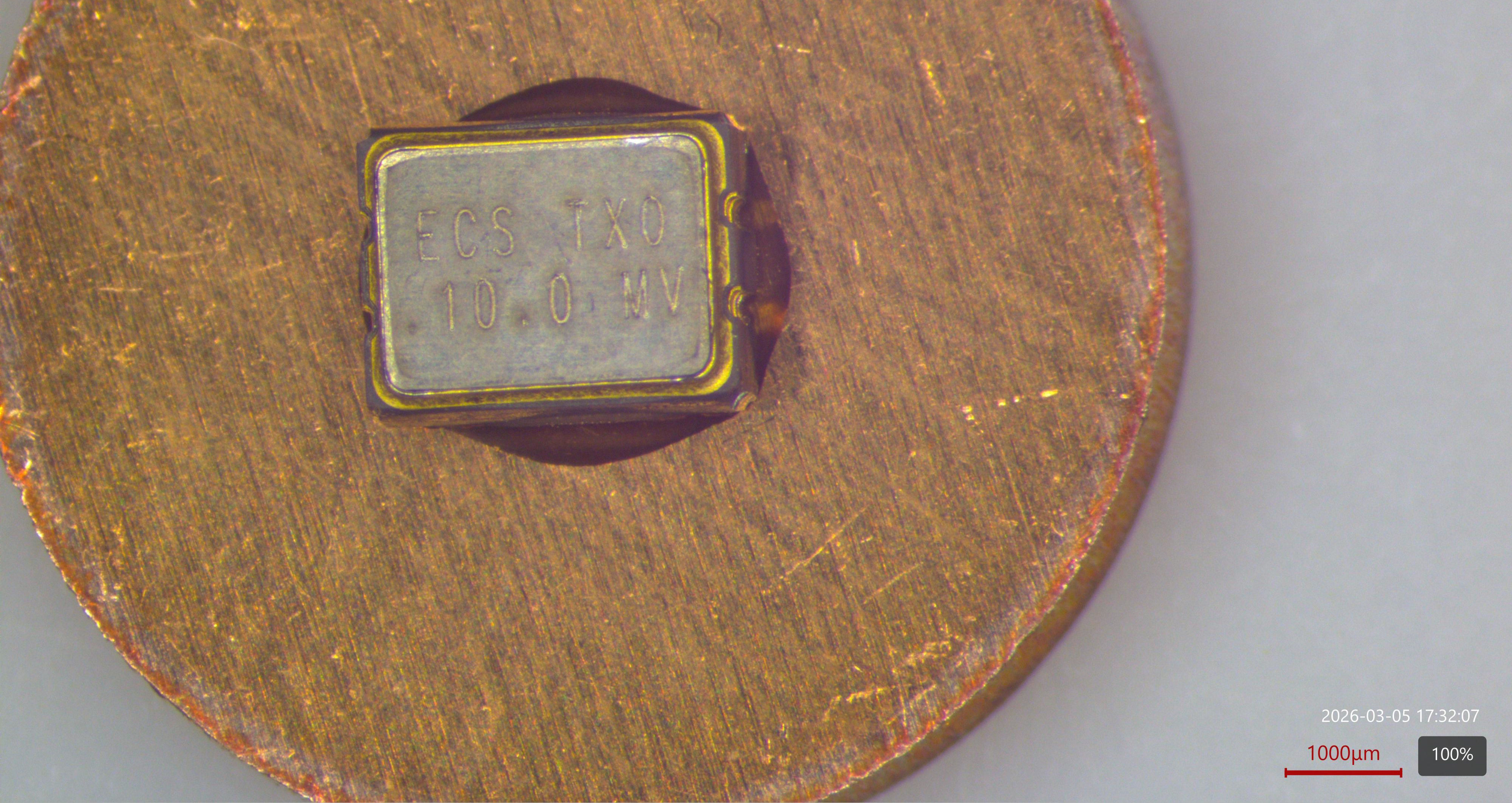
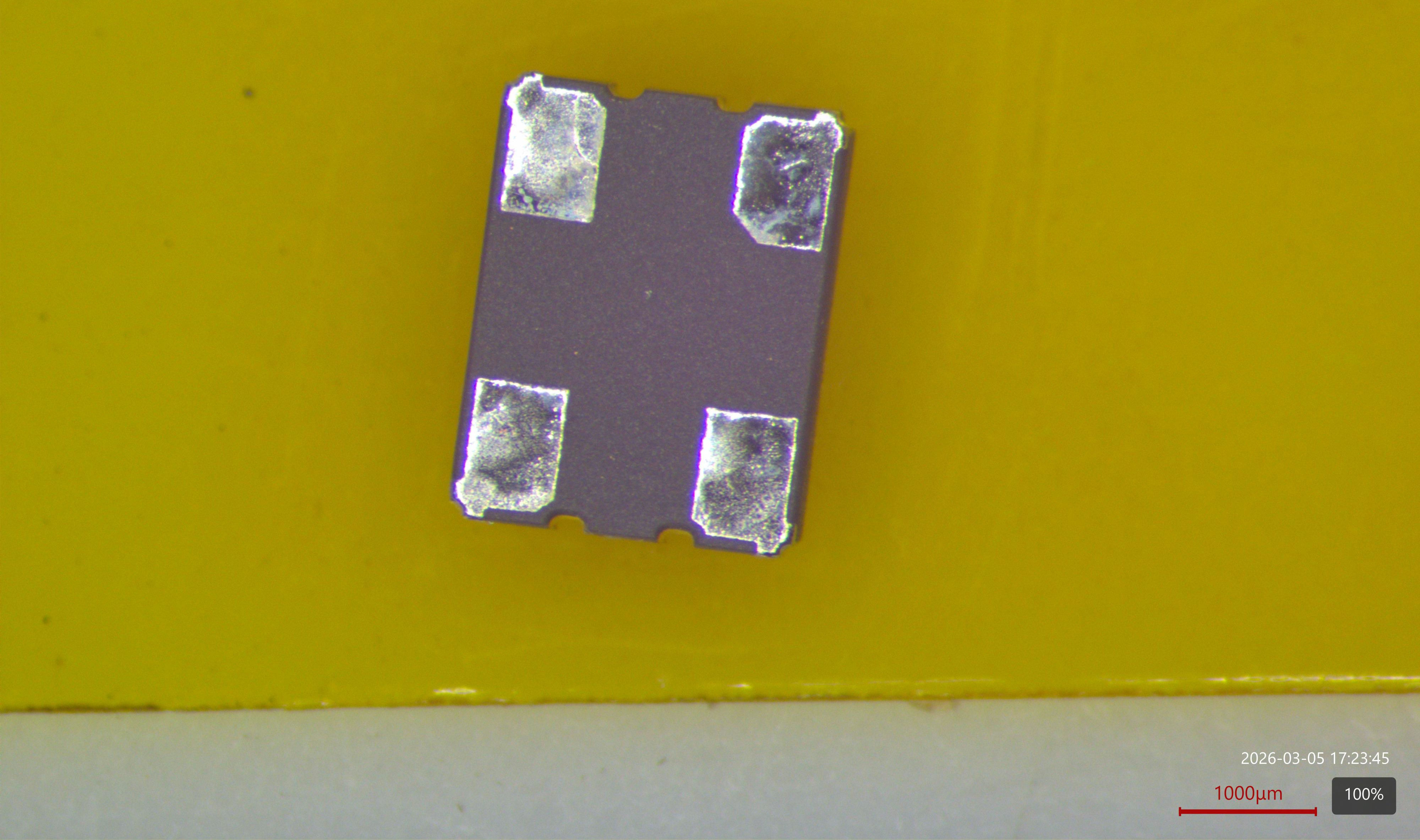
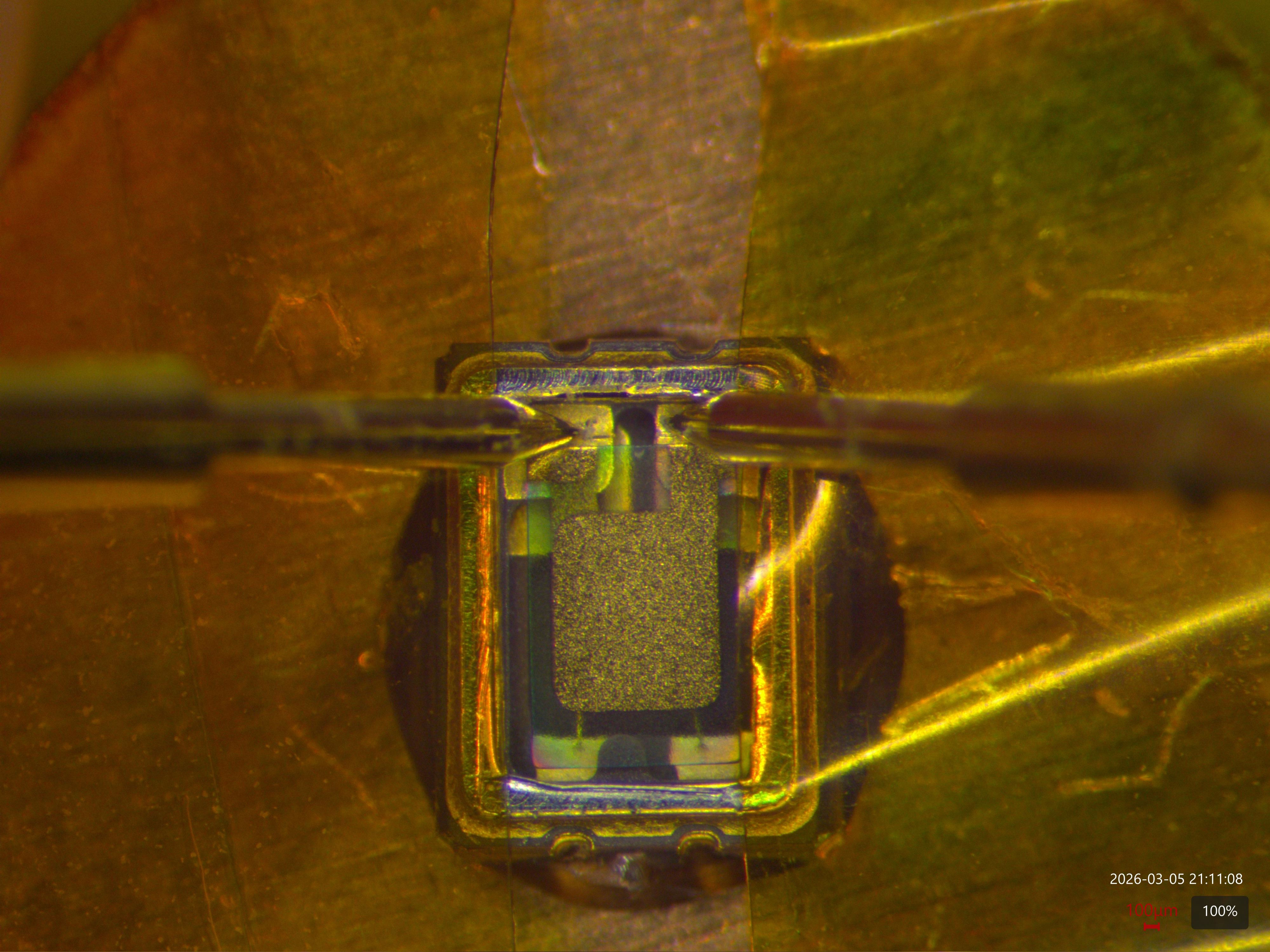
The TCXO is packaged in a 3.2 x 2.5 mm hermetically sealed ceramic package with a metal lid. It was externally unremarkable, with no visible damage.
Depackaging
I wasn’t sure how to decap it at first because I’m used to working with ICs encapsulated in standard black epoxy-glass molding compounds. I thought briefly about chemical methods, grinding, and machining before coming across MIL-STD-1580D section 12, which called for grinding or machining through most of the metal lid, thinning it down to the point that a handheld blade can make the final cut.
So I decided to try that.
I mounted the copper disk and TCXO up on my mill and started cutting. I probably could have made slightly faster progress if I swapped the 250 μm endmill out with a bigger one, say a 1.5 mm, but the sample was small enough I didn’t want to bother messing around with collets and wrenches to change tools. The machining only took a couple of minutes, making very slow gentle passes a few tens of μm deep before the edge looked to be about ready to punch through.
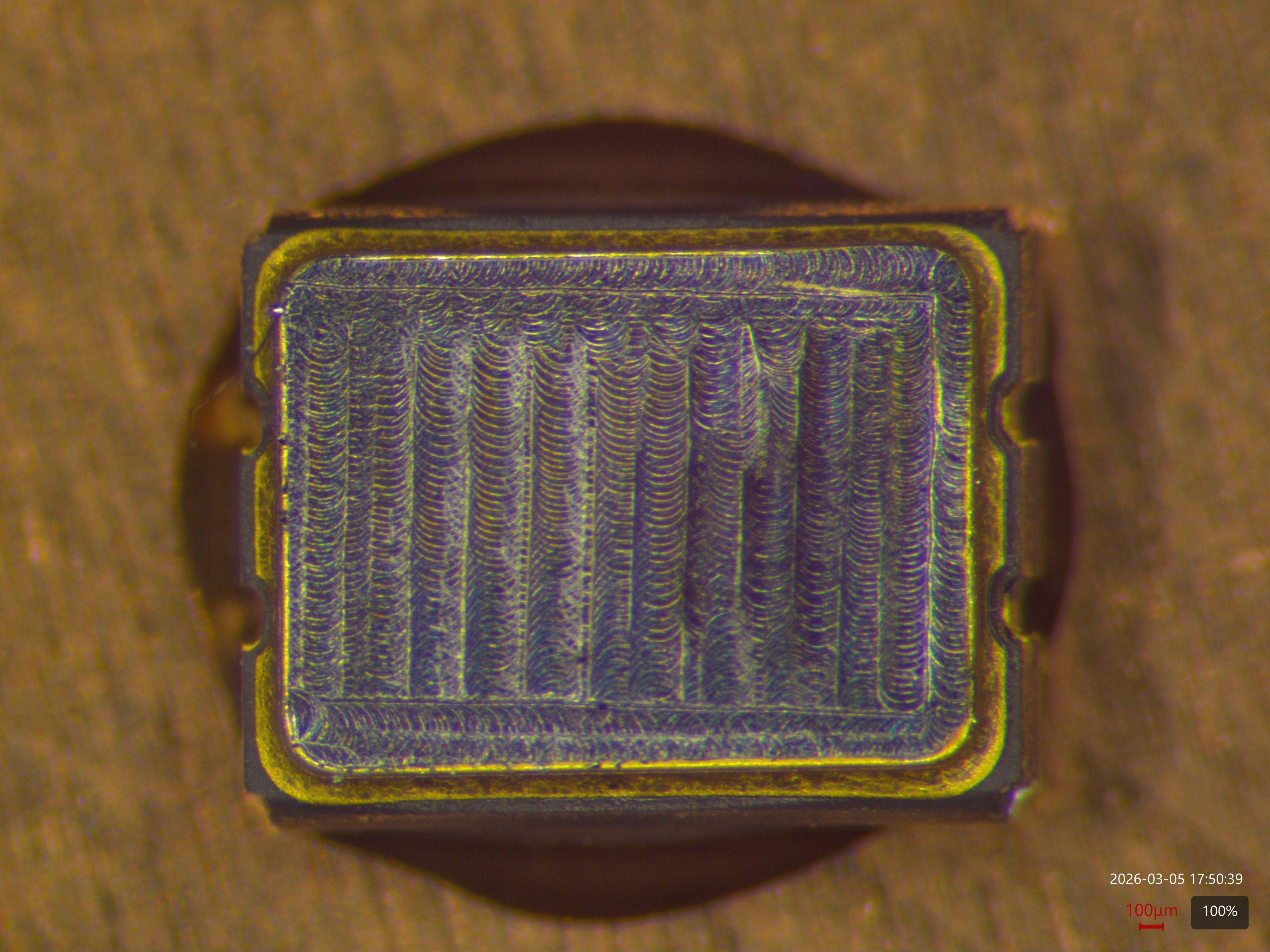
I took it off the mill, grabbed a #11 scalpel, and quickly cut a slit along two sides then began to lift up with the knife blade. After a bit of bending and tugging I was able to peel the entire lid off just like opening a tin can, without damaging the interior of the package or releasing any metal chips into it.
Visual inspection of quartz crystal
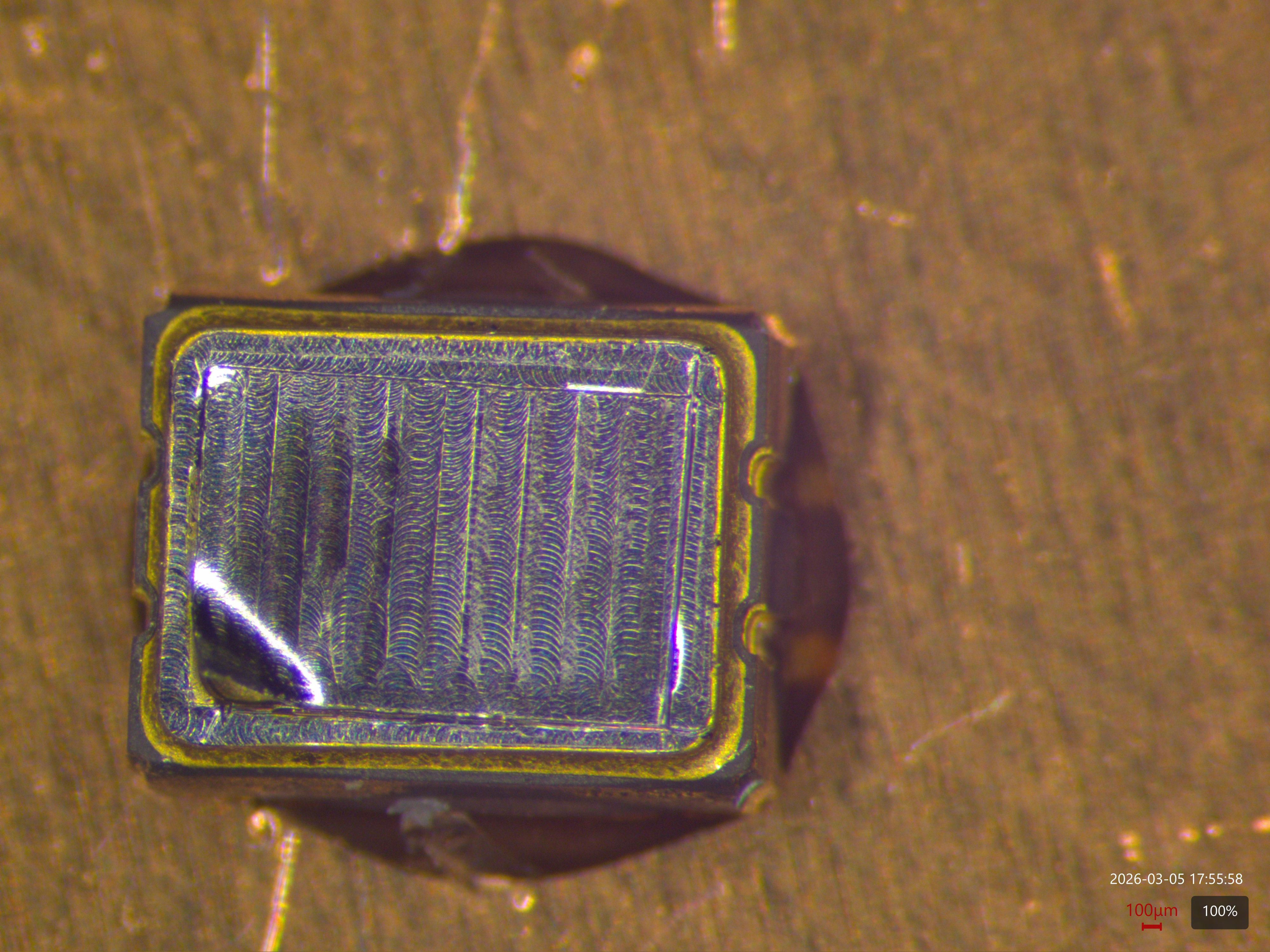
Now that the package is open, we can get a better idea of how the TCXO is constructed.
It’s actually a two level structure, the controller die is out of view on the lower layer (but we can see some gold contacts deep down that it presumably connects to). The quartz crystal is a rectangular sheet with a slightly textured surface and rounded corners, with a gold electrode covering most of the top and bottom surface. One side of the crystal hangs over a small rib on the edge of the package but doesn’t seem to touch it (maybe this is an end stop to keep it from breaking if dropped?) while the other side is attached to a pair of gold contacts on the ceramic package with a conductive adhesive of some sort, probably silver filled epoxy.
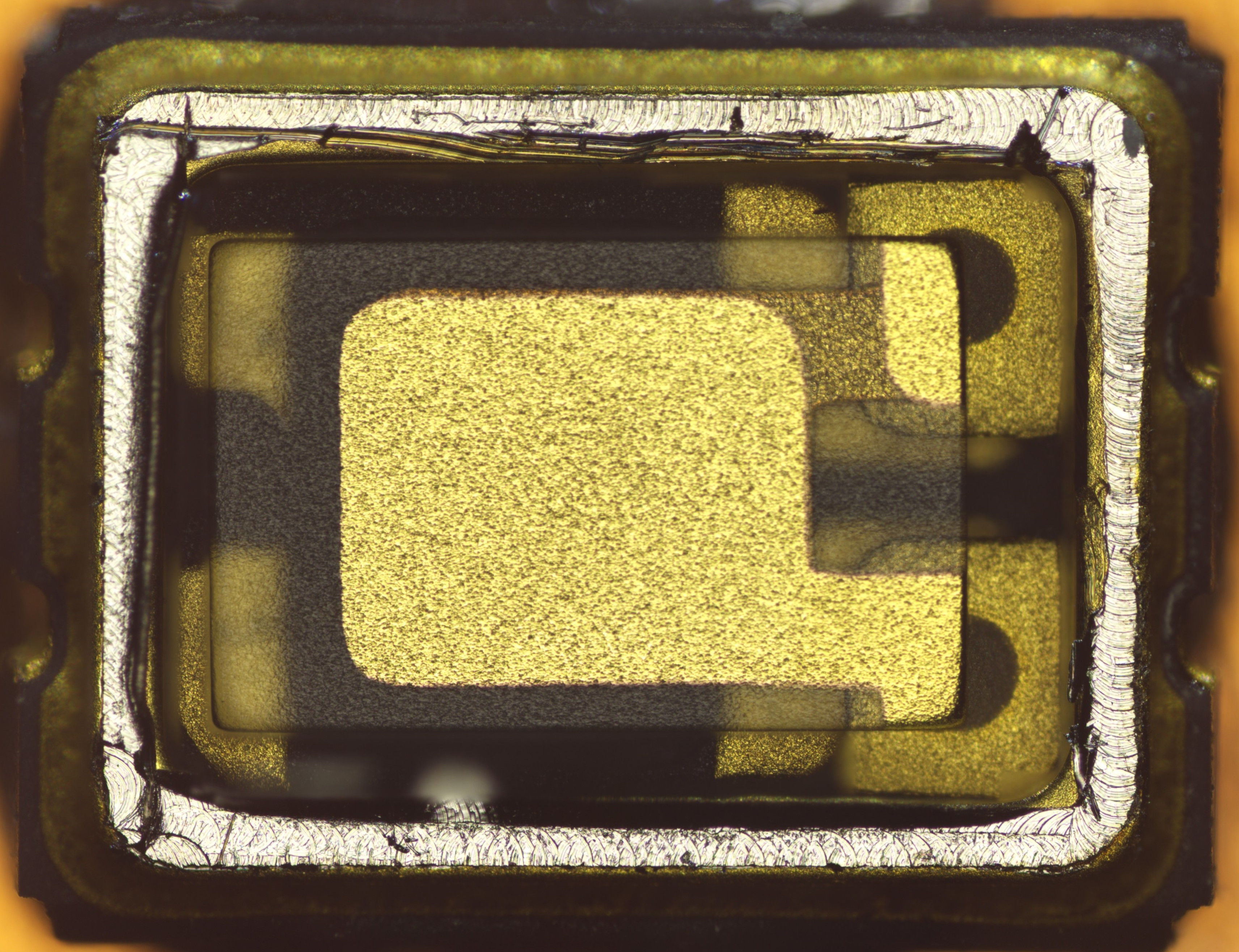
I spent quite a bit of time going over the entire surface of the quartz sheet with the 20x objective looking for any sign of fractures, chips, or damage, as well as inspecting both of the electrical connections from the crystal to the package for cracks or any sign of electrical defects. And I found nothing. This quite surprised me, because I expected the failure mode of a sonicated quartz oscillator to be “shake the resonator to pieces or rip it off the mount” and I was seeing nothing of the sort.
Electrical testing of crystal
I was gradually becoming less confident that the quartz crystal was the source of the failure, but any testing or analysis of the oscillator driver chip would require removing the crystal, potentially destroying it in the process (and, best case, destroying the connections between the crystal and substrate). So before taking that irreversible step, I wanted to do some electrical measurements of the crystal.
I did not have a proper fine pitch GSG probe or anywhere to land it, so I created a crime against metrology consisting of a pair of SMA cables off the front of the VNA, a pair of SMA to dual 0.1” pin header adapters (yes, these exist), a pair of single ended 0.1” extension wires, and a set of PCBite SP10 probes. It wasn’t the slightest bit impedance matched and I had no way to calibrate it (as a rough baseline, insertion loss was somewhere in the vicinity of -10 dB with the probes touching due to all of the reflections in the setup) but for narrowband measurements where I just wanted to check if the crystal was resonant or not, it would do.
After a bit of poking, I found what looked to be a textbook quartz crystal resonant curve, but centered at 20 MHz rather than 10. This suggests there’s a divide-by-two in the driver circuit, perhaps to improve the duty cycle to a more perfect 50%. But more importantly, it suggests that neither the crystal itself, nor the electrical connections between it and the package (since I was probing at the package contacts and not the surface of the quartz), were the source of the failure.

Removal of crystal
I was worried that the attachment between the crystal and the package would be super rigid and it would shatter during removal, but that turned out to not be the case. It was a soft, silver-filled adhesive that broke easily after getting a scalpel blade under the far edge of the crystal, allowing me to remove it with no visible damage under low magnification (perhaps some scratches visible at high mag depending on how hard the scalpel I used to pry it was compared to the quartz - hardened steel is around Mohs 7 which is the same as quartz, so depending on the exact alloy and hardening profile it may have been harder or softer).
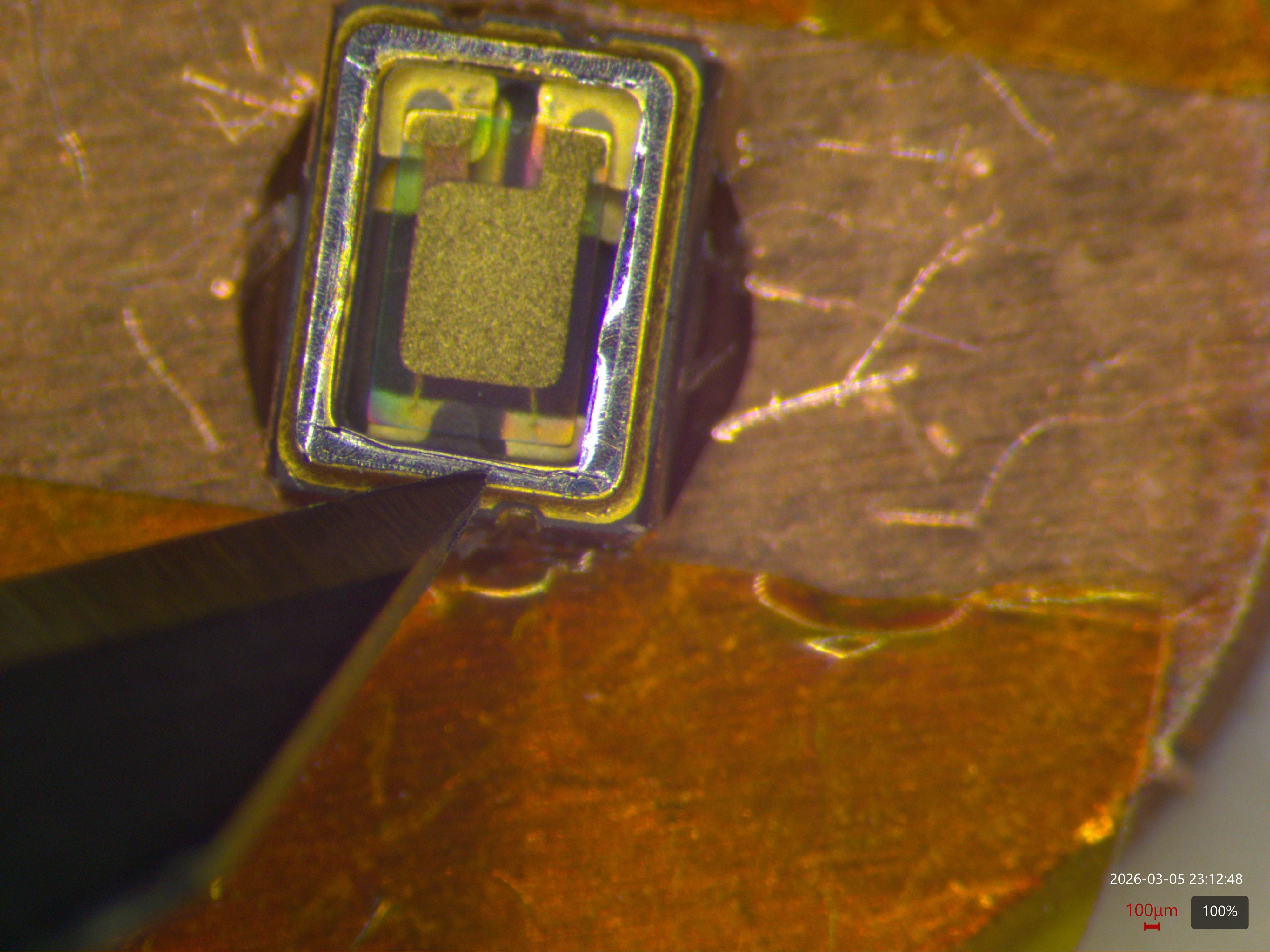
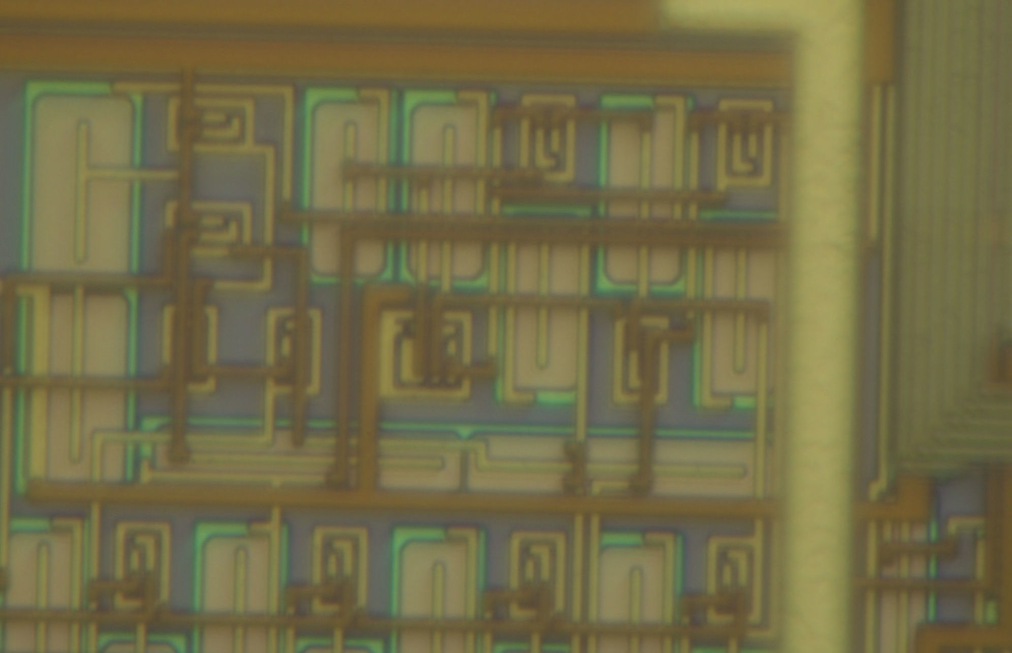
Controller visual inspection
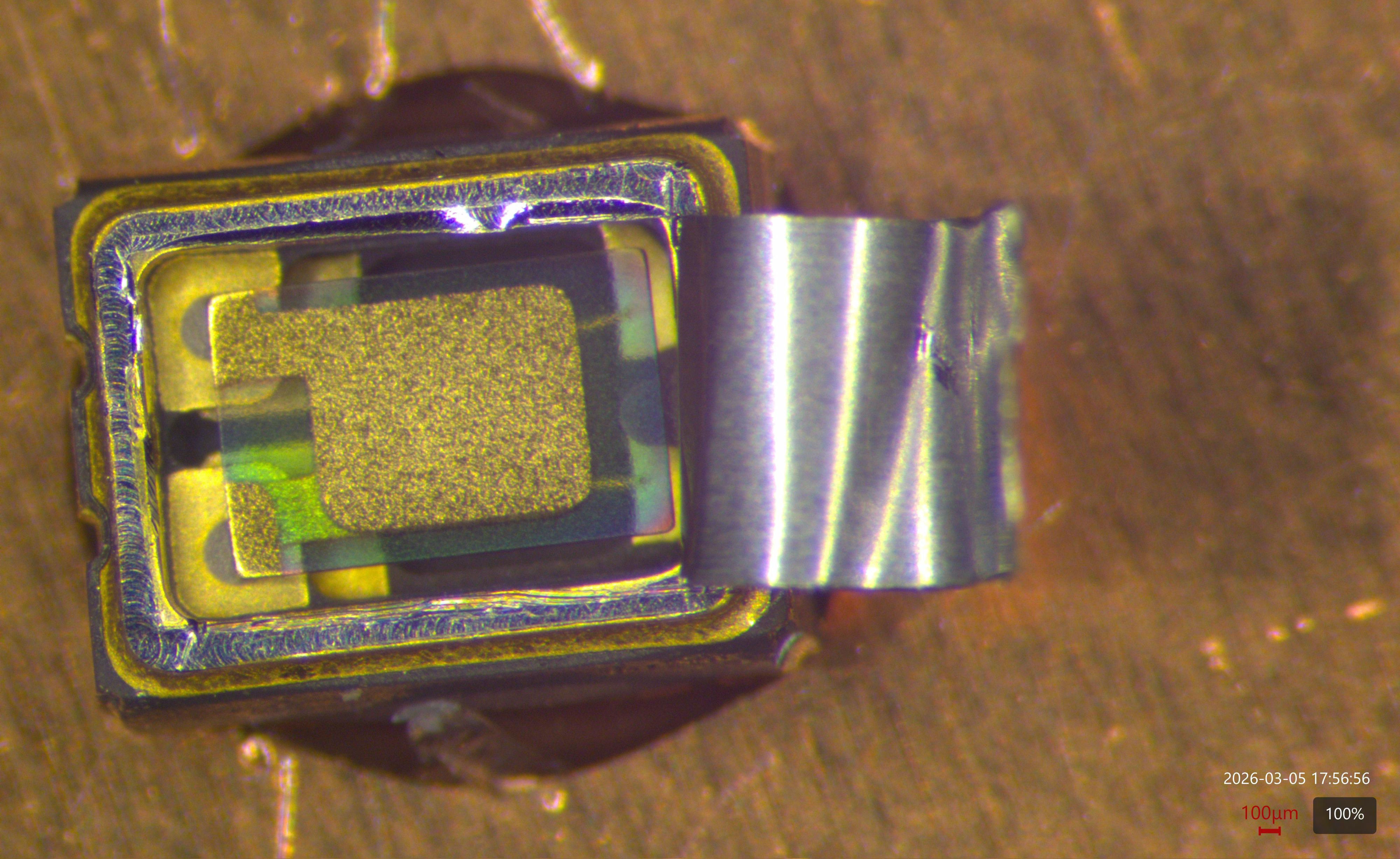
With the crystal out of the way, we see the package has three levels internally: the controller die (containing the oscillator driver, temperature compensation, and output divide-by-two) sits in a cavity at the lowest level, attached via a dark colored adhesive rather than the usual silver-filled epoxy (presumably because the package is not electrically conductive thus there is no point in using an expensive metal filled adhesive to ground the die backside).
The second level sits roughly flush with the top of the controller die, providing four electrical contacts on one side and two on the other that are connected to the six pins of the controller by gold ball bonds. I didn’t measure connectivity from these pads to package pins or the crystal, but based on the general floorplan of the device my educated guess is that the four corner pins connect to the package pins, while the two center pins connect to the quartz crystal (sitting above the controller on the third level).
The controller die has three bond pads on either side, which is not a match to the 4-and-2 layout of the package. As a result, one bond wire has to cross over the controller die to reach the far side of the package.
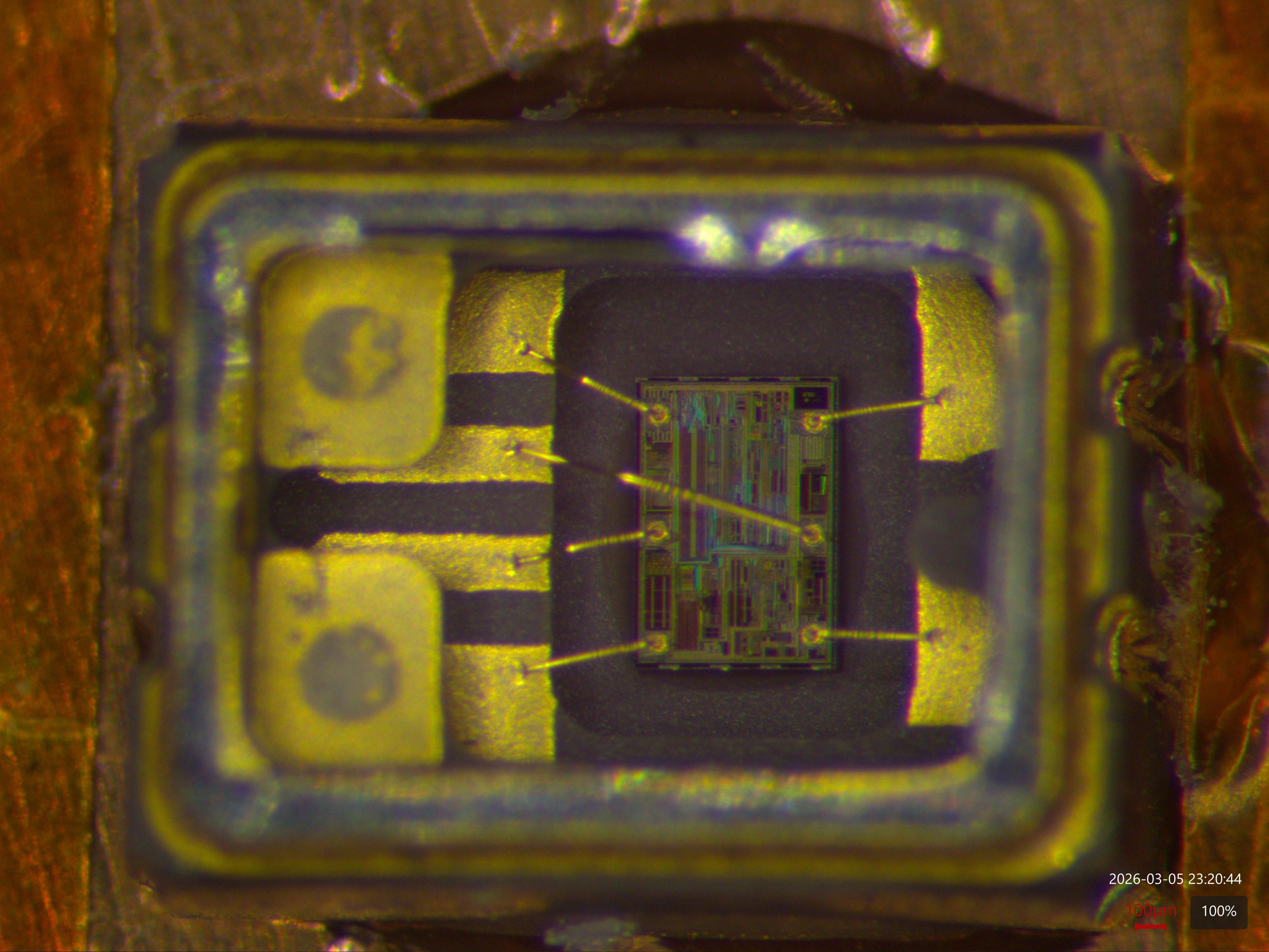
This photo is in the canonical orientation as shown in the datasheet, which means the southwest corner package pin is the output enable, then going counterclockwise we have ground, output, and Vdd.
All package pins measured plausible resistances to ground (a few hundred kΩ leakage measured with a Fluke 87V) as long as I had my microscope illuminator turned off. There was a strong photoelectric effect evident and I actually measured negative resistance on some pins with the LED ring light shining on the controller die. But this suggested that of the six bond wires, the ones going to the package pins were likely intact. By elimination, those going to the quartz crystal became my top suspects.
Controller die high magnification inspection
I couldn’t resist briefly putting on my IC reverse engineering hat to take a closer look at the controller die despite not seeing any obvious anomalies suggestive of an electrical failure (there was one bit I thought might be a burned trace but on closer inspection it was just a dust speck on the surface).
The controller die measures approximately 645 x 930 μm (0.6 mm^2) including scribe lines, and is made by Asahi Kasei Microsystems (a major supplier of TCXO controller ICs) according to the “AKM” logo in the northeast corner.
Counterclockwise from the southwest corner, the pinout is output enable, ground, crystal 1, output driver, Vdd, crystal 2. I was not expecting the outer seal ring to be OE (it’s ground in almost every device I’ve looked at) but I went back and double checked and I’m reasonably confident I had it correct. The northeast pad certainly looks like an output driver with the large interdigitated set of fingers on it.
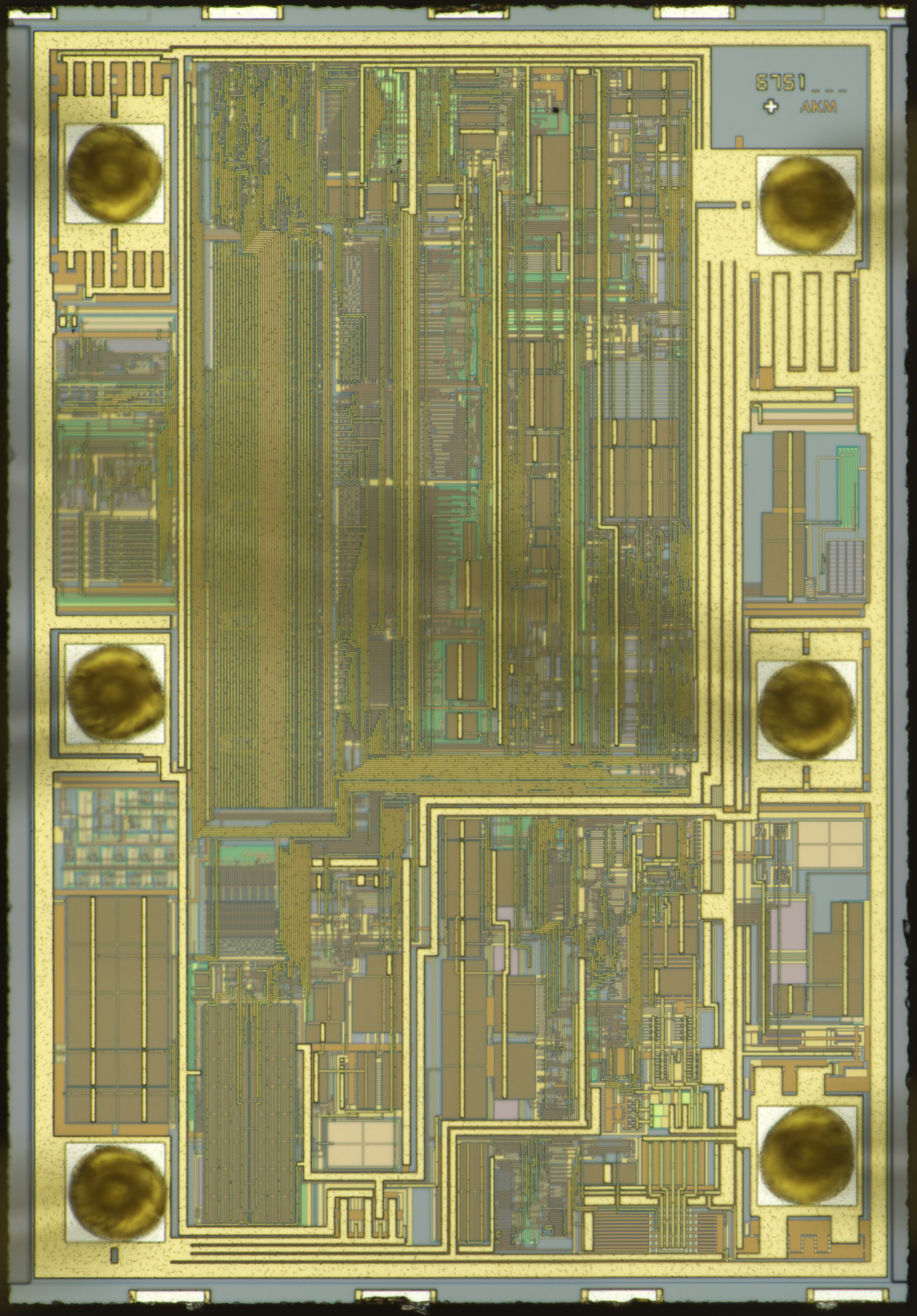
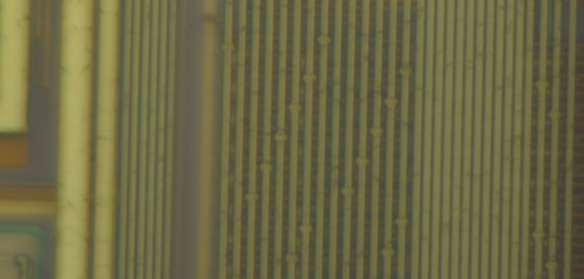
Looking at some of the analog areas which are less dense than the digital, it’s obvious that the device is made on a planarized process with three aluminum metal layers. The three metal layers show up as a light straw color, a darker brown, and another light straw color although it is easy to disambiguate metal 1 and 3 by depth of focus at high magnifications. A greenish layer is also visible below metal 1, likely polysilicon.
Minimum metal 1 feature size is around 660 nm with a 1225 nm pitch, metal 3 has larger 940 nm features with around 1400 nm pitch (however, overglass likely makes the wires on M3 appear fatter than the actual metal features are). M3-M2 vias do not have any visible sagging in the metal trace, but can be easily identified visually by a roughly 2000 nm circular capture pad on the conductor. Standard cell rows are about 9.9 μm tall, consistent with a technology node around 250 nm.
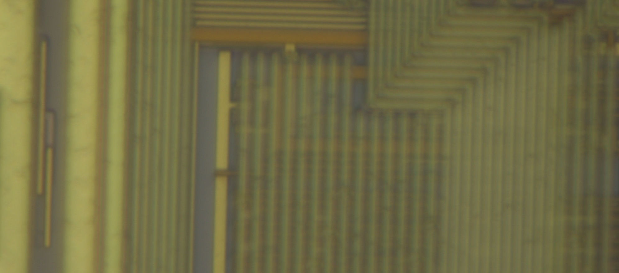
I’m far from an expert at reading analog VLSI layout so I didn’t dig deeper - I can recognize some structures like large capacitors (big solid colored rectangles on lower layers) and polysilicon resistors (long skinny squiggles on the green layer), but didn’t attempt to deprocess the device or do extensive reverse engineering.
Bond wire inspection
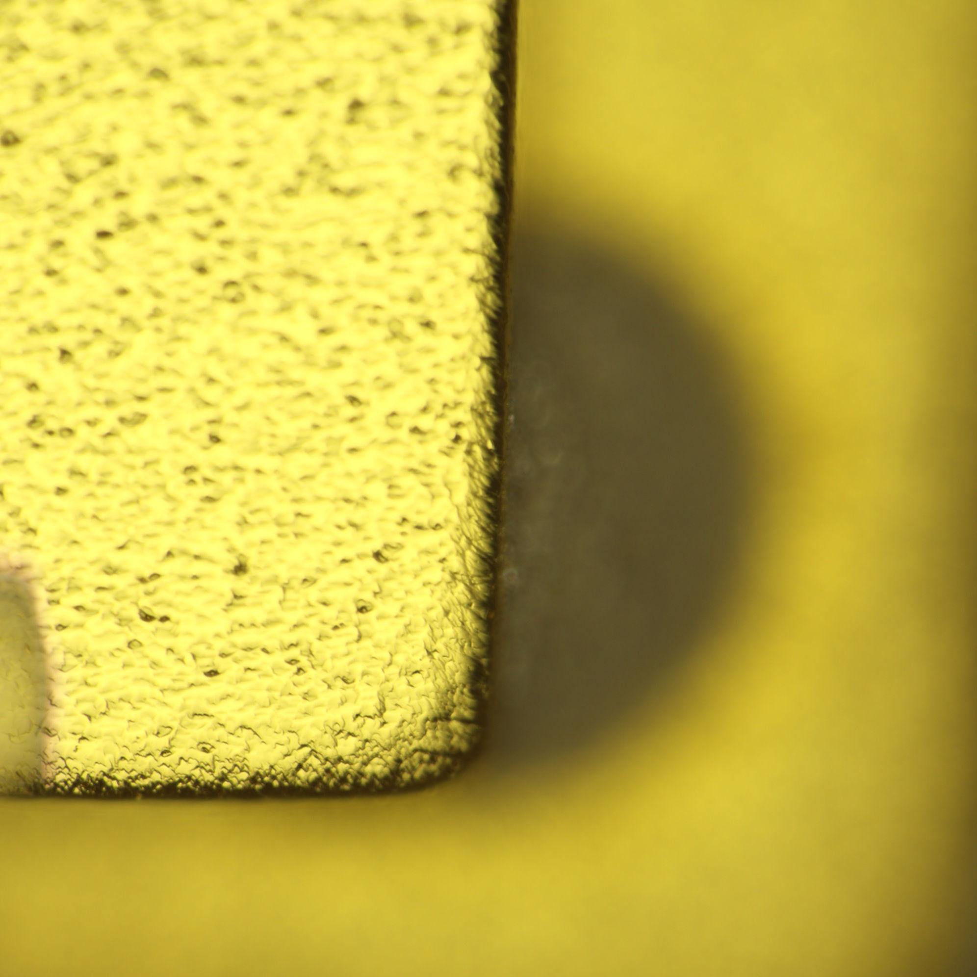
With that detour out of the way, it was time to look at the last remaining suspect: the bond wires. It pretty much had to be one of the two bonds from the crystal to the controller, since the crystal itself appeared to be resonating fine, and the connections from the controller to the package pins appeared intact.
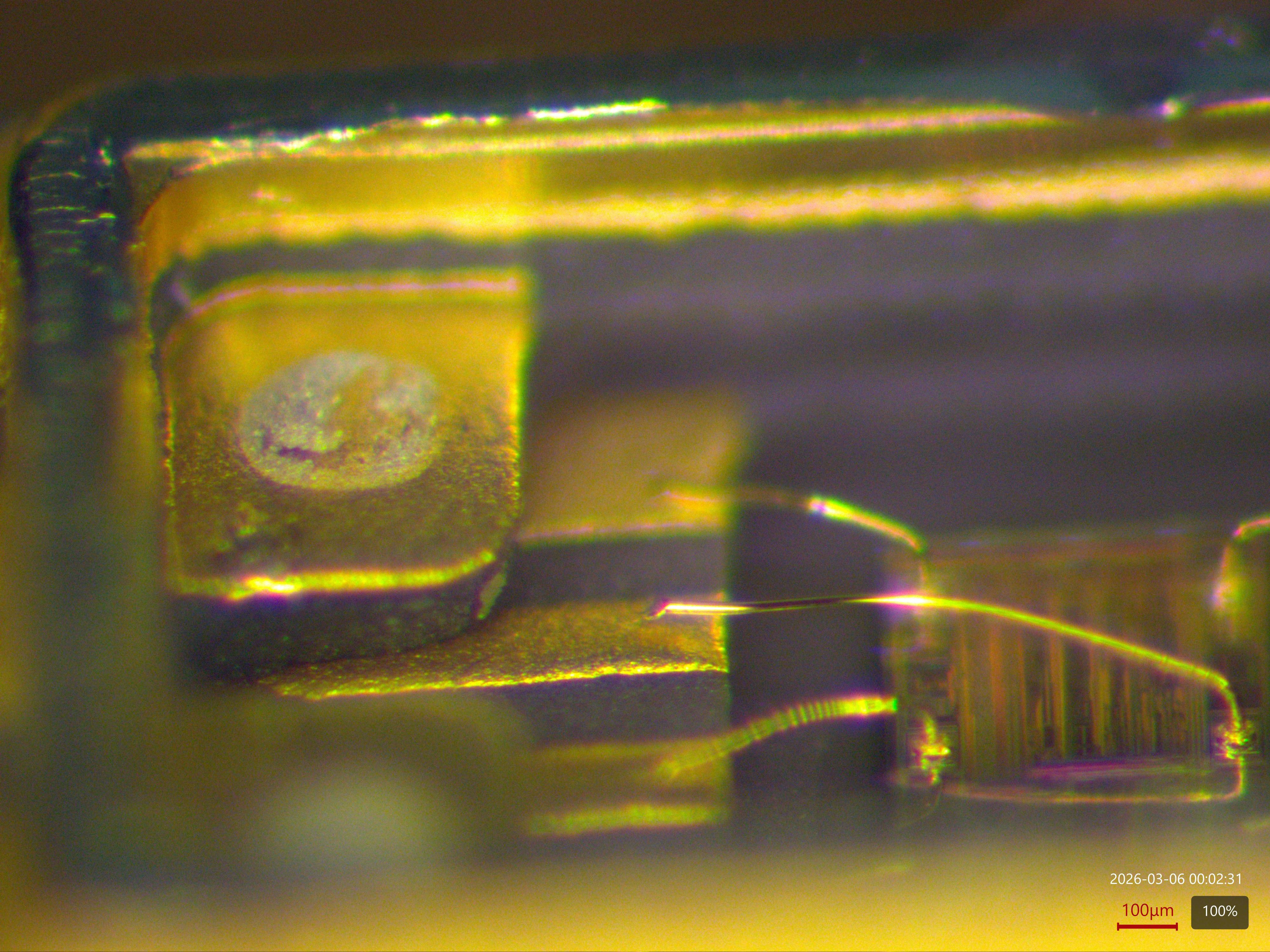
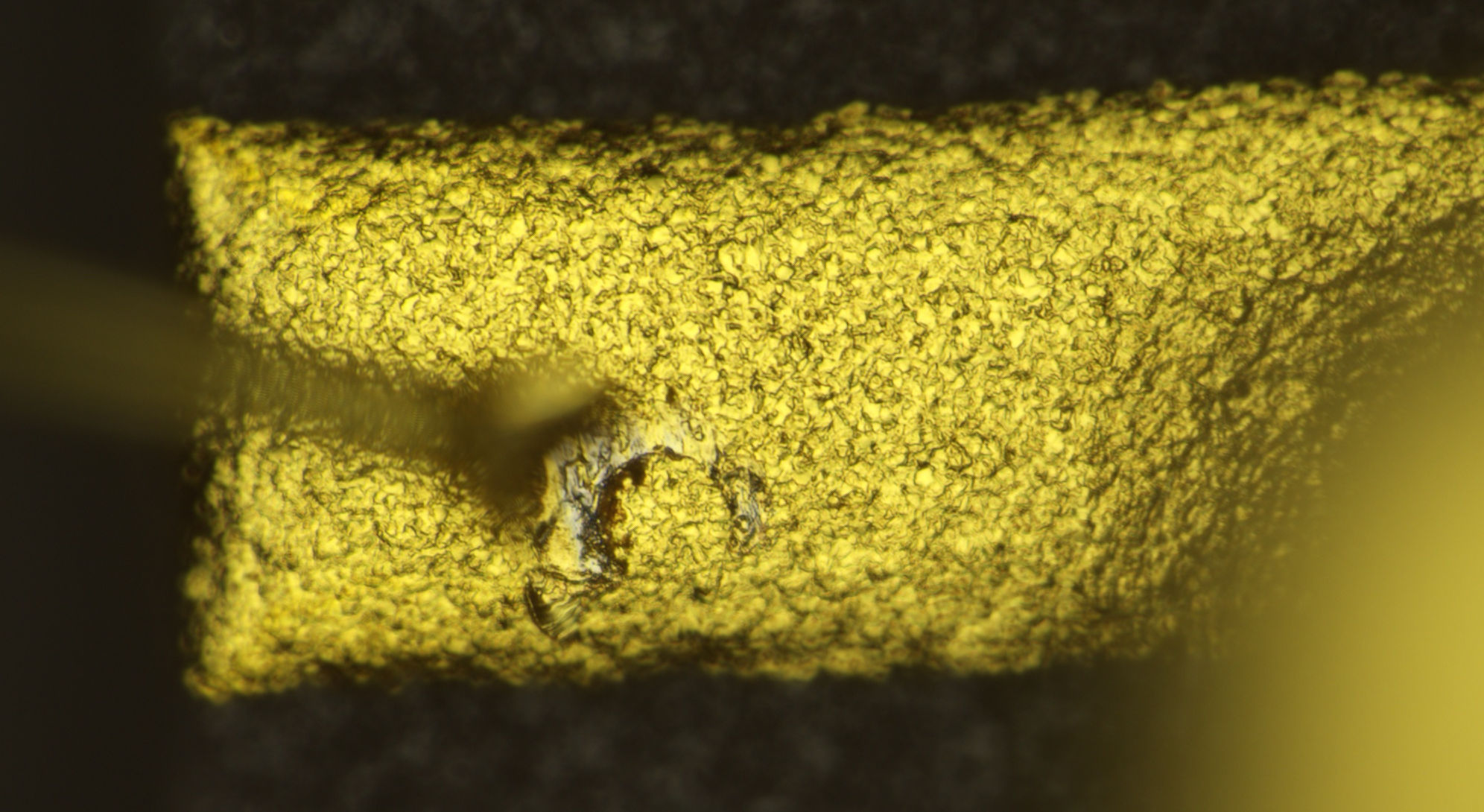
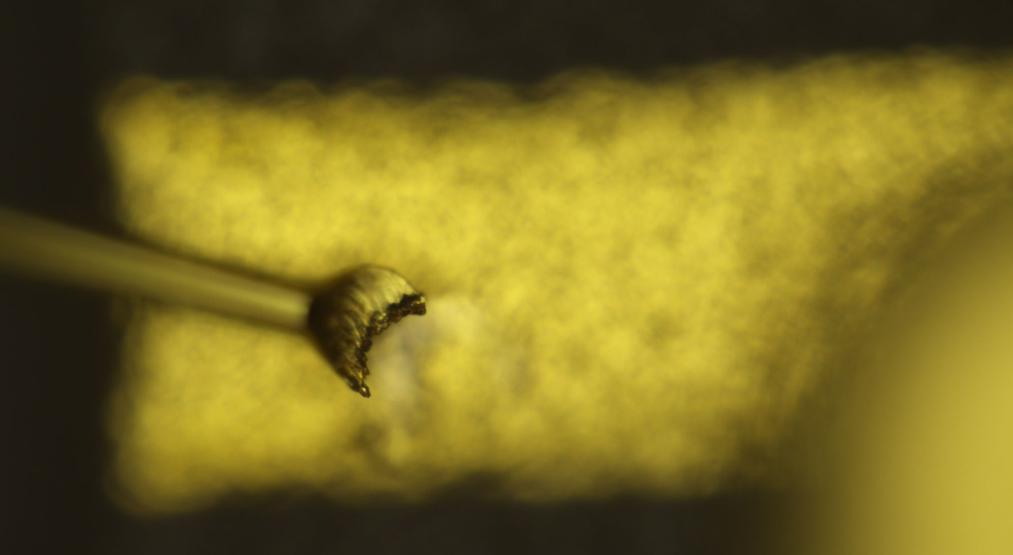
Sure enough, I found a broken crescent bond on the long bond wire crossing over the controller die, right where it should have connected to the package.
Under the stereo microscope at a shallow angle the wire was visibly floating above the pad, but it was a lot more visible in the eyepieces (with proper depth perception) than in the still photo.
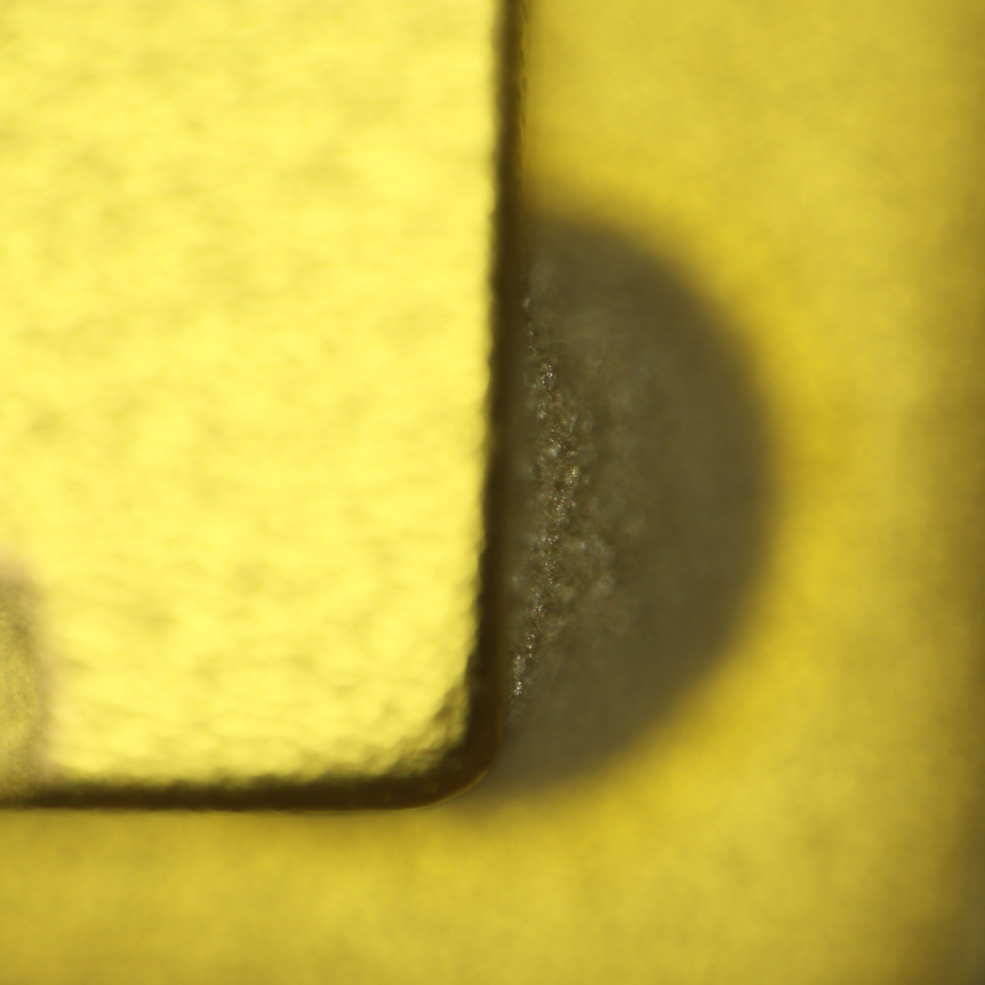
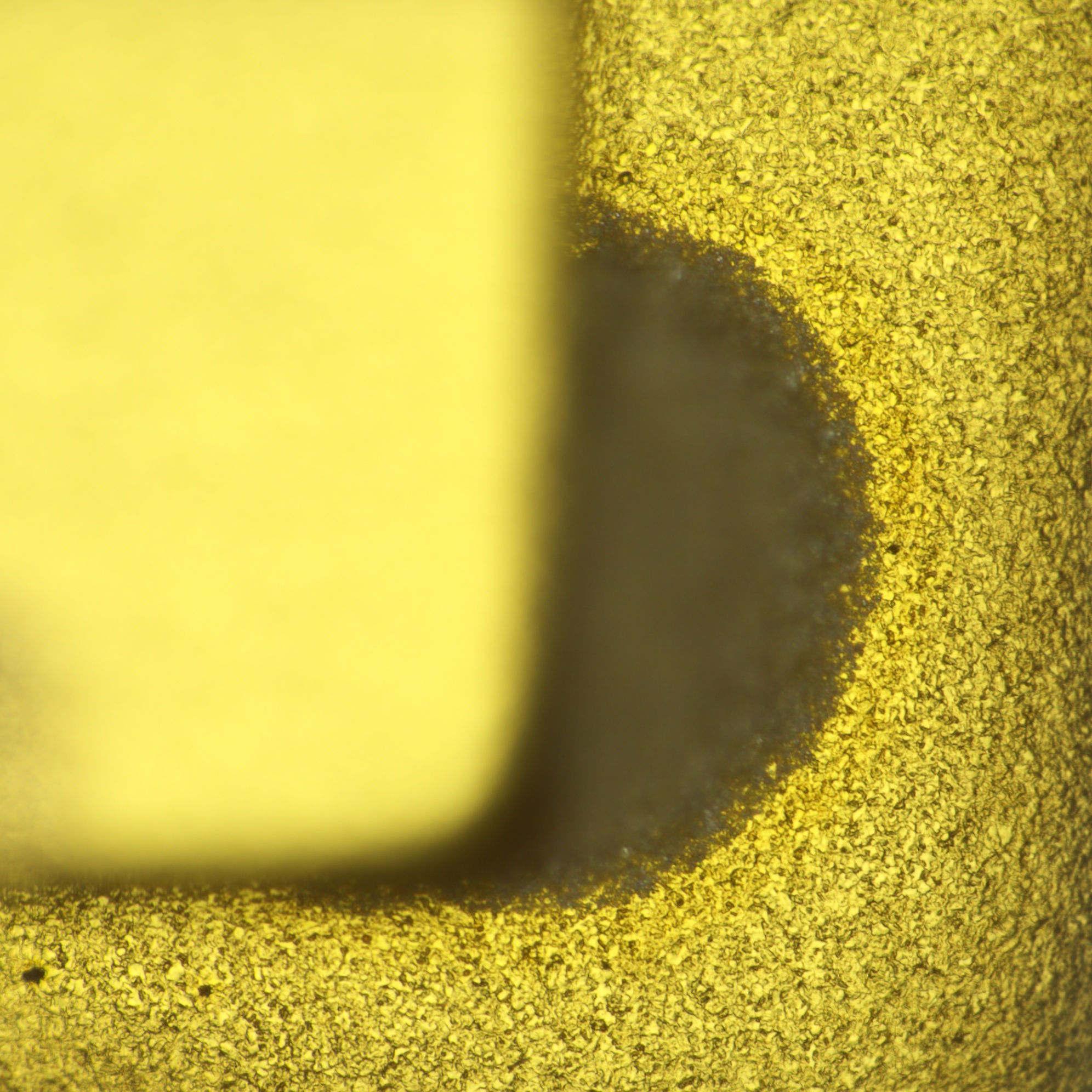
Switching to the metallurgical microscope in a top-down view, looking at a good bond first, we can see a rough textured surface on the gold contact pad, with the gold wire coming in from one side and compressed into a crescent shape by the ball-bonding capillary (hence why some sources refer to the second bond as a “crescent bond”). The gold wire and gold pad appear to be well connected, and a deep circular indentation is visible in the pad which goes through the gold into a silvery base metal.
I’m not an expert at wire bonding although I’ve done lab scale gold ball bonding before so I understand the basics of the process and I’ve never seen this deep an indent before. Could this be an indication of too much pressure or ultrasonic power? Would love comments from people who actually run high volume bonders as to whether this is indicative of poor process control, it sure seems fishy to me.
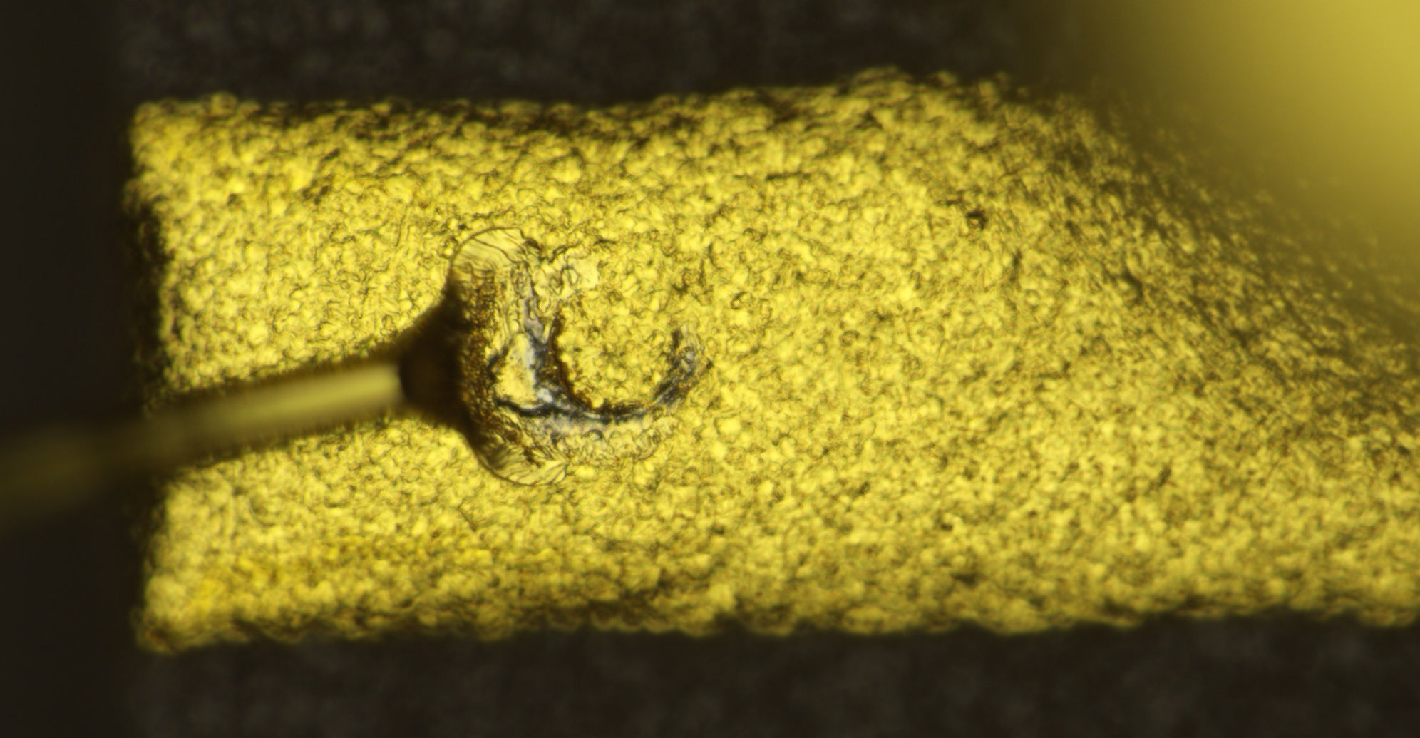
Looking at the long bond from the controller to the crystal, it’s clearly fractured at the wire to package interface.
Conclusions
The failure of the TCXO was the result of the long bond wire between the controller die and the substrate trace connecting to one side of the quartz crystal separating from the package at the crescent bond interface. Sonication of the part and poor process control of the wire bonding process were likely both contributing factors.
After finishing the lab work and while writing this blog, Aleksorsist told me she had seen a second case of the same failure mode - TCXO failing with flatlined output after ultrasonic cleaning during rework. I don’t have the failed part and it may have been scrapped already, but that’s pretty strong evidence that the sonication was a contributing factor.
Like this post? Drop me a comment on Mastodon